AI Perception Gap: Atomic Architects — How AI Is Redesigning Our Physical World
The Materials We Desperately Need
Material Dreamland
Imagine a world where long-distance power lines lose no energy, electric cars charge in seconds, quantum computers hum away in every research lab, and frictionless, levitating trains zip between continents at blistering speeds. Discovering a room-temperature superconductor, a material referred to as the ‘holy grail’ of physics, would be nothing short of revolutionary. But achieving it isn’t just about genius scientists in labs; it’s increasingly about AI working alongside them to redefine the limits of materials science.
Suppose a researcher were to imagine a shopping list of desired properties for a material capable of transforming an entire industry (e.g., plastic that biodegrades quickly). Could AI design the desired material’s atomic structure, use a digital model to prove the material has the desired properties, and even produce the material in the real world? In the paragraphs ahead, we’ll explore how academics and pioneering companies at the forefront of materials science are transforming our physical world with AI.
What is a superconductor?
Firstly, a conductor is a material that allows electric current to flow. As you may recall from physics lessons at school, electric current is essentially the movement of electrons — however, this movement isn’t perfectly efficient. As electrons travel through a conductor — like the copper wiring found in household electrical circuits — they sometimes collide with vibrating atoms in the material. These collisions cause some of the electrical energy to be converted into heat — this is known as electrical resistance. The longer the wire, the more collisions occur, and the more energy is lost as heat.
A superconductor, on the other hand, is a special type of conductor in which this energy loss does not occur. The phenomenon was first discovered in 1911, when Dutch physicist Heike Kamerlingh Onnes cooled solid mercury to -270°C and observed that its electrical resistance disappeared entirely. Since then, scientists have identified various materials that become superconductors when cooled below a specific threshold, known as their critical temperature.
Why would a room-temperature superconductor be transformational?
A room-temperature superconductor is a material that offers zero electrical resistance in ambient conditions. The material doesn’t need to be cooled to extreme temperatures or operate at a demanding air pressure for electrical resistance to vanish. Such a development has immense potential, especially in our transition to a renewable energy grid.
We’ve designed our energy system to keep the wires short: move the fossil fuels close to the cities, burn them there, and distribute the electricity locally.
With renewables, we cannot transport sunlight and wind to city-based power plants in the same way we can fossil fuels. We are instead forced to create electricity in the deserts, oceans, and mountain ranges rich with renewable sources. The primary obstacle to achieving a fully renewable grid is not the availability of natural resources, but the challenge of transmitting electricity over extremely long distances. Electrical resistance at that scale is not just inefficient; it’s a dealbreaker.
Room-temperature superconductors would change this entirely. Electricity could travel thousands of kilometres without any loss. We could harness solar power from the Sahara, wind in the North Sea, hydro in the Alps, and transmit it all over Europe without waste. It’s not just an upgrade — it would be a redefinition of what’s possible in global energy systems.
And that’s just one application of one material. A room-temperature superconductor could revolutionise computing, transportation, energy storage, and healthcare, to name a few. All the while, material scientists are hunting for many other transformational materials, such as biodegradable packaging, high energy density batteries, and self-cleaning surfaces (to repel contaminants in medical implants).
Materials Science
To understand how we could discovery breakthrough materials like these, we turn to materials science — a field that blends physics, chemistry, and engineering to explain why materials behave the way they do. Materials scientists study how atoms respond to forces or environments depending on their arrangement. This understanding allows us to achieve specific functions for materials by tailoring the arrangement of atoms.
Of particular importance are stable materials, often called crystals. Stability is linked to the energy required to break bonds or trigger chemical changes. Material stability is crucial because unstable substances degrade, deform, or react unpredictably, limiting their usefulness in engineering and design.
Think of a stable material as a calm person in a crisis — someone who stays composed even under pressure, heat, or chaos. The person who remains calmest is considered the most stable. In materials science, the most stable materials are prized for everything from spacecraft to smartphones. These are the materials that scientists hope to discover.
Discovering New Materials
Trial, Error, and Centuries of Waiting
At the field’s inception, materials scientists discovered new materials through trial and error. Early ironworkers discovered that iron, when heated in charcoal, became stronger and harder. The heating process caused carbon from charcoal to diffuse into the surface of iron, leading to the production of primitive forms of steel. This discovery occurred during the Iron Age (long before atomic structure of a material could be understood), with evidence of steel production found in Anatolia (modern-day Turkey) as early as 13th century BC.
As the field progressed, materials scientists used intuition to develop new materials. For instance, if a certain oxide had useful properties, they’d try similar oxides with other elements. Further, materials were often discovered by subjecting elements to extreme conditions, in terms of temperature and pressure, and observing unexpected behaviors.
From the late 19th century, microscopic technology allowed scientists to see microstructures and atomic arrangements. These helped correlate structure with properties, for example, why certain alloys were tougher or more malleable.
Computational Methods
Following the introduction of the computer in the 1950s, computational materials science garnered increasing attention. By the 1970s, scientists were able to predict the properties of solid-state materials digitally using an algorithm called density functional theory (DFT). Given the atomic structure, scientists could understand the material without having to physically create it in the real world.
Initially, the electronic, magnetic, and chemical properties of simple materials could be predicted using DFT with relative ease. As computational power increased, materials scientists began modeling the behavior of far more complex substances. A landmark example of DFT’s impact was its accurate prediction of the exceptional electronic properties of silicon. This insight fueled a surge of research in the 1980s — and now, silicon is at the heart of the memory and processing chips in the device you’re using to read this blog.
AI Unleashed: The Discovery Explosion
Google DeepMind (introduced in AI Perception Gap: Unlocking Biology’s Secrets with AlphaFold) is working at the cutting edge of this field. Its AI model, GNoME, identified 2.2 million potential crystal structures — unique atomic arrangements predicted to be stable. Of these, 380,000 are classified as highly stable. For context, humans discovered around 20,000 stable crystals through experimentation since early pioneers discovered steel in the Iron Age. Computational methods later expanded our stable materials universe to 48,000. GNoME has nearly tenfolded this number, taking us past 400,000 — massively boosting our chances of finding breakthroughs like a room-temperature superconductor.

Although promising new materials can be identified at scale with technology, synthesising them in the real world is often challenging and time-consuming. As of November 2023, scientists had produced 736 of the 421,000 candidates shared by DeepMind. That may seem like a drop in the ocean, but it marks meaningful progress. Thanks to digital tools that estimate how promising a material might be, researchers can prioritise only the most likely successes for real-world synthesis.
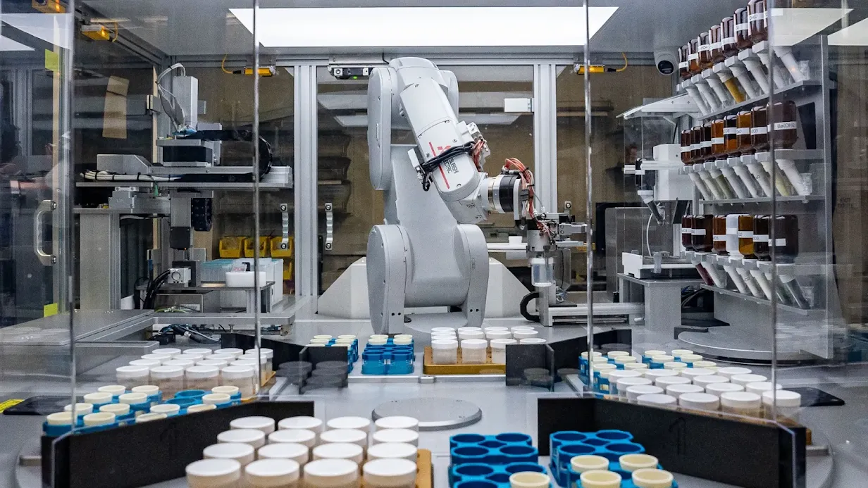
Even more impressively, robots are now helping turn theory into reality. At Berkeley Lab’s A-Lab, AI-driven robots work 24/7 to create materials in powder form in the real world. The lab begins by selecting candidate compounds identified through AI tools at Google DeepMind and other organisations. Language models (think ChatGPT) trained on vast materials science corpora then generate detailed experimental protocols. Then, robotic systems follow these recipes in fully automated workflows — measuring, heating, mixing, and analysing compounds with machine precision. In a published study, A-Lab reported synthesising 41 out of 58 materials in 17 days.
Let that sink in: AI dreamed up a material that never existed, predicted how it would behave, devised the instructions to synthesise it in our physical world, and then guided a robot to bring it into existence.
The Age of Inverse Engineering
With advancements being made from research groups and innovative companies around the world, inverse design is set to become the pinnacle of computational materials science. The desired properties — like high electrical conductivity, thermal stability, or optical transparency — are declared first, then AI selects the elements from the periodic table and the required structure to achieve the list of desired properties.
I invite the reader to spend 70 seconds listening to Pushmeet Kohli, VP of Science Research at Google DeepMind, discuss this vision.
Conclusion
Okay, I am well over 100 hours deep of blog writing and I’m getting tired. It’s time for AI to write an entire paragraph in my final edition of my AI blog. I’m going to put my feet up.
From early blacksmithing to autonomous laboratories, the journey of materials science has always been shaped by the tools at our disposal. Today, AI and robotics are radically accelerating that journey — unlocking not just the promise of room-temperature superconductors, but a wide array of transformative innovations. We’re designing self-cleaning surfaces that repel contaminants in medical implants, high energy density batteries that could reshape electric mobility, and biodegradable packaging to address global sustainability challenges. The ability to explore millions of materials digitally — and rapidly test the most promising ones in the real world — means that breakthroughs once considered speculative are edging toward inevitability.
Thank you for your input, ChatGPT. Well, this post wraps up my six-part series AI Perception Gap. I invite the reader to reflect on their experience by reading my closing remarks here.
Enjoy Reading This Article?
Here are some more articles you might like to read next: